Leave A Message
Leave A Message
Fill out the form with your requirements and quantities(PCB/ Component Sourcing/ PCBA), and upload your Gerber file & BOM list. We'll provide you with a free quote as soon as possible!
submit
banner
Home

PCB Layout

PCB Layout

What is PCB Layout ?

PCB Layout (Printed Circuit Board Layout), referred to as PCB Layout or PCB Design, is a vital part of the electronic product manufacturing process. It involves the electronic components in accordance with the predetermined circuit diagram design for a reasonable arrangement and connection, so as to form a functionally complete, stable performance of the printed circuit board (PCB). PCB layout is not only the placement of components, but also involves the wiring, heat dissipation considerations and electromagnetic compatibility and other aspects.


DQS ELECTRONIC has highly-skilled teams to find right solution for complex design problems, our teams of designers are qualified engineers with over 10 years of experience, also are experts of design through PADs PowerPCB, OrCAD, and more, DQS ELECTRONIC have designed many types of boards range from the consumer electronics, industrial, medical, military, and telecommunications industries, the design capability runs from small samples to large & complex circuit boards.


And our value-added services (SI \ EMC \ PI \ Thermal analysis \ DFM analysis, etc.) as the main core competence, supplemented by EMS manufacturing as a professional one-stop solution service system. We offer these products at reasonable prices to the great satisfaction of our clients.


Reliable Designs We Can Provide 

—— IPC class 2 and 3, JEDEC and MIL standards are available ——

  • #


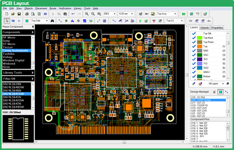
    • Single/double sided /Multilayer:through via hole, blind/buried via and laser via technologies.

    • Flexible / flexi-rigid printed circuits.

    • HDI Designs with micro vias and advanced materials – Via-in-Pad, laser micro vias.

    • High speed, multi layer digital PCB designs – Bus routing, differential pairs, matched lengths.

    • PCB Designs for space, military, medical and commercial applications

  • #


    • Extensive RF and analog design experience (printed antennas, guard rings , RF shields…)
    • Signal integrity issues to meet your digital design needs (tuned traces, diff pairs…)
    • PCB Layer management for signal integrity and impedance control.

    • DDR, DDR2, DDR3, DDR4, SAS and differential pair routing expertise

    • High density SMT designs (BGA, uBGA, PCI, PCIE, CPCI…)

  • #
     

    • Blind & Buried via ,Flex PCB designs, flexible rigid board of all types.

    • Low level analog PCB designs .

    • Ultra low EMI designs for MRI applications.

    • Complete assembly drawings.

    • In-Circuit Test data generation (ICT)

    • Drill, panel and cutout drawings design.

    • Professional fabrication documents creation.

    • Autorouting for dense PCB design.


We always try our best to offer options to reduce costs, to provide you with value engineering.
Fill out the form with your requirements, and we’ll be in touch soon.

Custom Order Request

submit
leave a message
If you are interested in our products and want to know more details,please leave a message here,we will reply you as soon as we can.
submit

Our hours

24H

Contact Us: Sales@dqspcba.com

home

products

WhatsApp

Contact