Leave A Message
Fill out the form with your requirements and quantities(PCB/ Component Sourcing/ PCBA), and upload your Gerber file & BOM list. We'll provide you with a free quote as soon as possible!
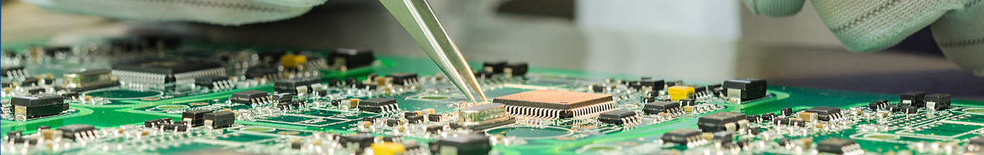
HDI PCB Capability
| Item | Capability |
| 1+n+1 | Yes |
| 1+1+n+1+1 | Yes |
| 2+n+2 | Yes |
| 3+n+3 | Yes |
| 4+n+4 | Yes |
| Any-layer | Yes |
| Laser hole diameter max | 0.15mm |
| Laser hole diameter min | 0.075mm |
| Laser Blind hole thickness to diameter ratio (max) | 1:1 |
| Laser Blind Hole Plating Filling | Yes |
| Laser Blind Hole Resin Plug Hole | Yes |
| Stack via | 3 step |
| Stagger via | 3 step |
| Filling via dimple value | <=15um |
| Laser via capture pad size | 0.25mm |
| Laser via hole size | 0.1mm |
| Laser via land pad size | 0.3mm |
| Minimum spacing between laser hole edge to laser hole edge (Same Net) | 0.1mm |
| Minimum spacing between laser hole edge to laser hole edge (Different Net) | 0.25mm |
| Max finished hole size for blind & buried via | 0.25mm |
| Minimum spacing between laser hole edge to buried drill hole edge (Same Net) | 0.2mm |
| Minimum spacing between laser hole edge to buried drill hole edge (Different Net) | 0.4mm |
| Minimum spacing between laser hole center to board edge (Inner layer) | 0.4mm |
| Minimum spacing between laser hole center to board edge (Outer layer) Stamped/Routed edge | 0.35mm |
| Minimum spacing between through VIA hole edge to PADs (Outer layer) (Different Net) | 0.175mm |
| Min thickness to Internal layer | 0.075mm |
| Max. dielectric thickness | 0.2mm |
| Min. dielectric thickness | 0.06mm |
Email :
Sales@dqspcba.com
We are committed to building a world-leading circuit board assembly service brand, providing customers with the most reliable products and support, setting a benchmark in the industry and promoting the development of the electronics industry.


Our hours
24H

 IPv6 network supported