Leave A Message
Fill out the form with your requirements and quantities(PCB/ Component Sourcing/ PCBA), and upload your Gerber file & BOM list. We'll provide you with a free quote as soon as possible!
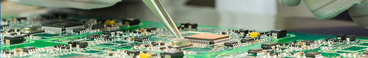
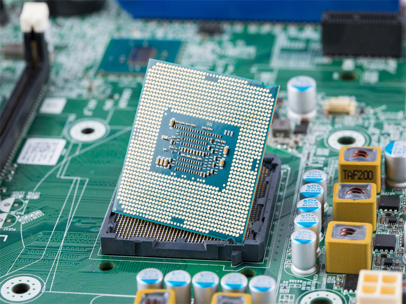
BGA Assembly
BGA(Ball Grid Array) is a surface-mount packaging technology primarily used for integrated circuits. In BGA packaging, the leads at the bottom of the package are shaped into balls and arranged in a grid-like pattern, which allows for connection to the pads on a circuit board. This type of packaging offers several advantages, including higher pin density, better heat dissipation, and lower inductance compared to traditional packaging methods such as DIP (Dual In-line Package) or QFP (Quad Flat Package). The BGA assembly process typically involves precise placement and soldering of the BGA package onto the circuit board, often using automated machinery to ensure accuracy and efficiency. The assembly may also include steps such as cleaning, inspecting, and testing to ensure the quality and reliability of the final product.
BGA Capability
Dense grid arrays up to 35×35 mm package size
Min ball space between 0.3 mm and 0.5mm
I/O counts up to 1500 pins
Support high speed routing on PCB top layer
Advantages of BGA Technology
BGA technology allows for a higher number of pins to be accommodated within the same area compared to traditional packaging methods.
This makes it possible to achieve higher integration and smaller chip sizes, contributing to the miniaturization and slimming down of electronic products.
The short and evenly distributed pins in BGA packages reduce signal transmission path lengths, resulting in lower parasitic inductance and capacitance.
This minimizes signal attenuation and distortion, ensuring signal integrity and stability, especially in high-frequency signal transmission scenarios.
BGA packages provide better thermal impedance between the package and the PCB, allowing heat generated by the integrated circuit to be more easily conducted to the PCB.
The array of solder balls acts as a heat dissipation channel, enhancing the chip's stability and lifespan by effectively reducing hot spot temperatures.
The relatively large pin spacing and self-alignment characteristics of BGA packages make them easier to assemble using standard SMT equipment.
This improves the reliability of the welding process and reduces the risk of assembly defects.
The absence of external pins reduces the risk of pin breakage or bending, enhancing the overall reliability of the package.
The solder ball array structure can distribute stress, allowing BGA packages to operate stably in complex environments.
BGA technology is compatible with a variety of materials and design requirements, making it suitable for different applications.
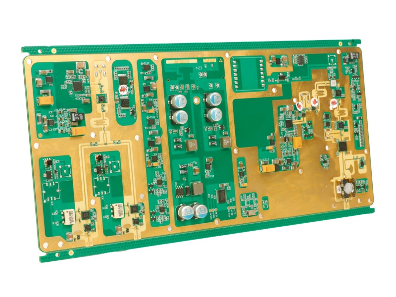
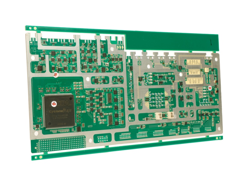
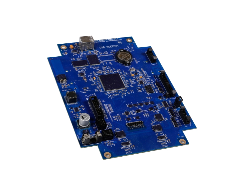
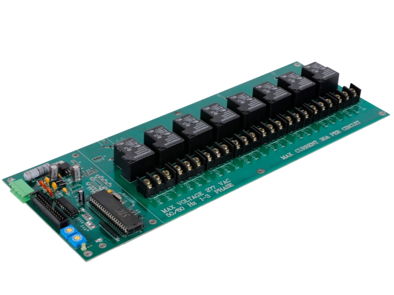
BGA PCBA Project
Email :
Sales@dqspcba.com
We are committed to building a world-leading circuit board assembly service brand, providing customers with the most reliable products and support, setting a benchmark in the industry and promoting the development of the electronics industry.


Our hours
24H

 IPv6 network supported