Leave A Message
Fill out the form with your requirements and quantities(PCB/ Component Sourcing/ PCBA), and upload your Gerber file & BOM list. We'll provide you with a free quote as soon as possible!
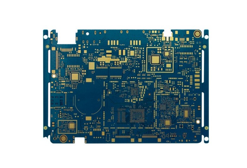
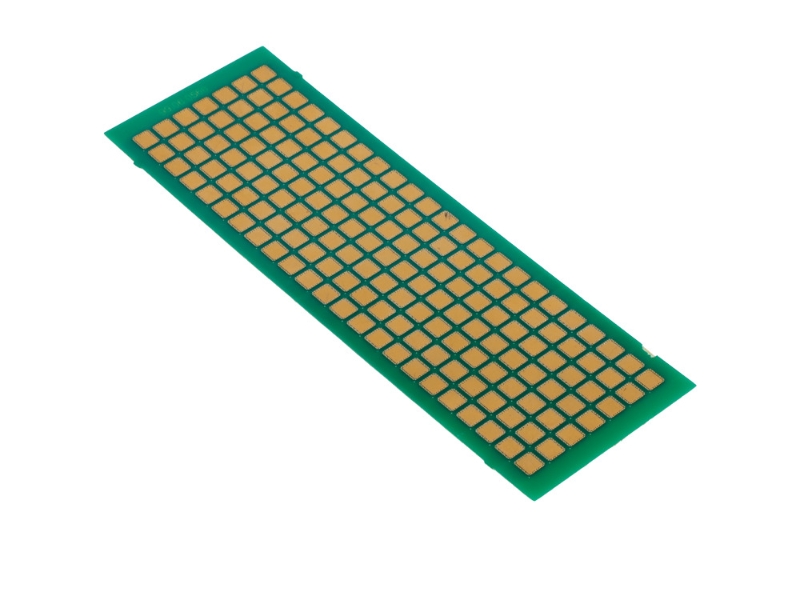
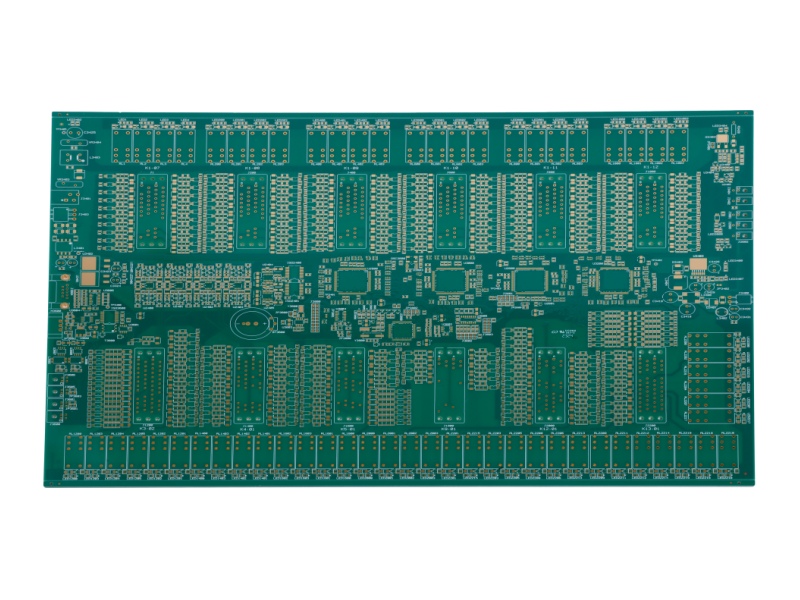
Layer :
6Material :
TG170Board Thickness :
1.2mmMin Line Width/Space :
0.1/0.1mmSurface Finish :
Immersion GoldApplication :
CommunicationCertificate :
UL&IPC Standard &ISO


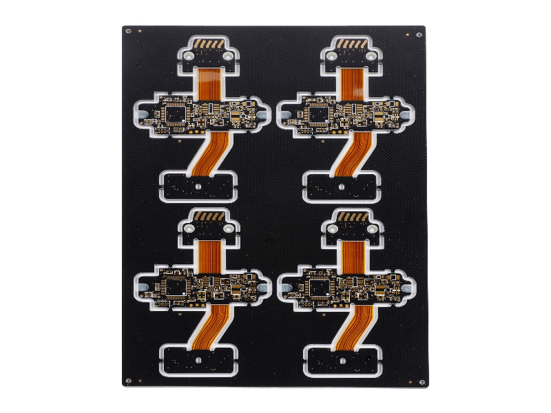
What Is HDI PCB?
HDI(High Density Interconnector) printed circuit boards are high-density interconnections with high circuit distribution density using manufacturing processes such as micro-blind technology, lasers, electrchemical hole filling, and stacking methods.
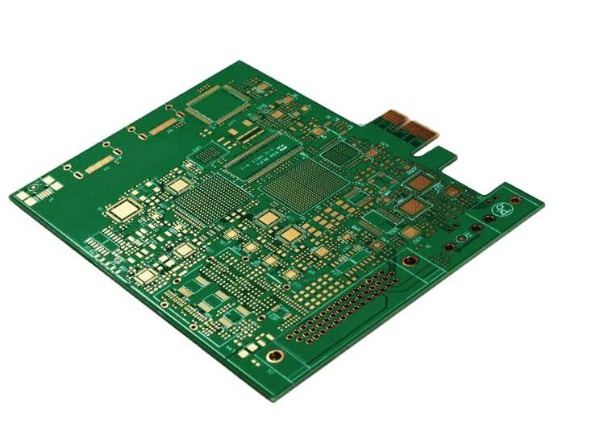
HDI PCB Advantage:
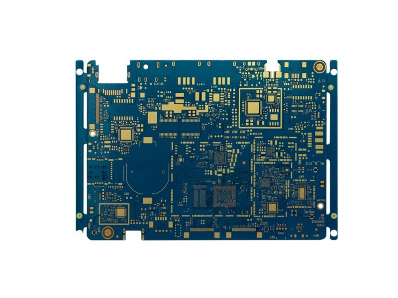
High density: Compared with traditional PCB boards, HDI boards have a higher wiring density, which effectively improves the complexity of circuit design and reduces the size of the product.
High reliability: HDI boards have excellent heat resistance, humidity resistance and electrical properties, ensuring the long-term stable operation of electronic equipment.
Excellent electrical and thermal properties: HDI sheet has a low dielectric constant and low coefficient of thermal expansion, which effectively improves the transmission speed of electrical signals and ensures the stable operation of electronic equipment in various environments
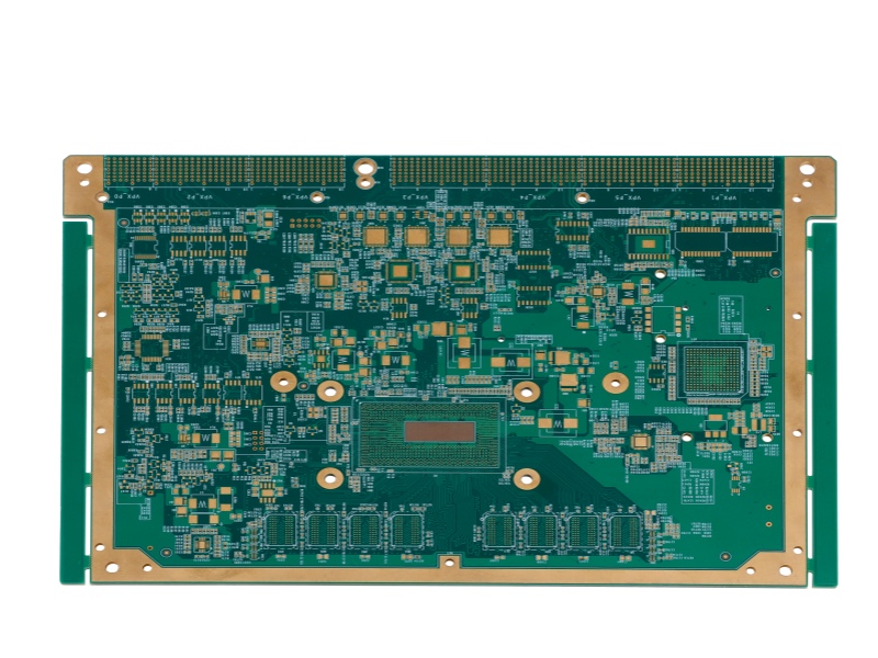
Application:
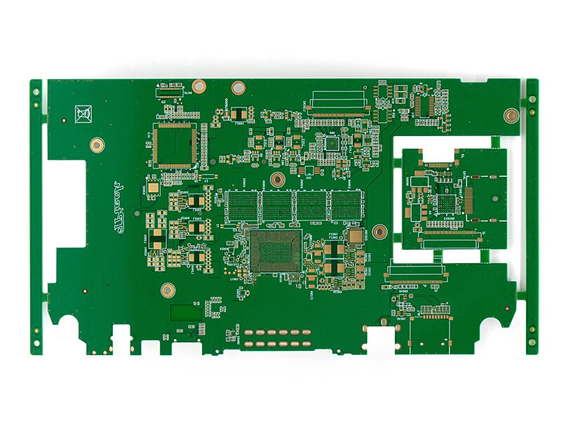
HDI printed circuit boards are widely used in communication equipment, computers, consumer electronics, automotive electronics, and other electronic devices to meet the needs of high-speed data transmission, multi functionalintegration, and small-size design in these fields. It is also widely used in medical equipment, aerospace and defence due to its high wiring density and high reliability.
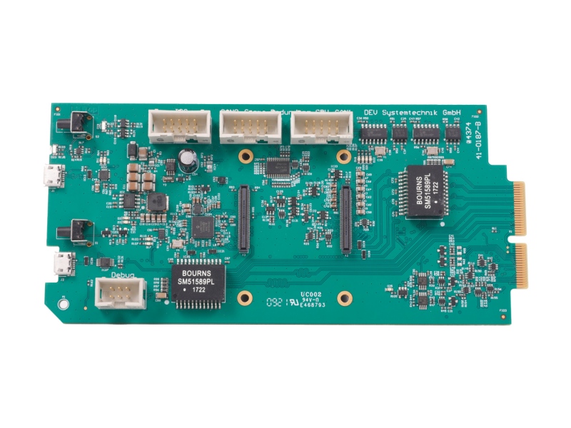
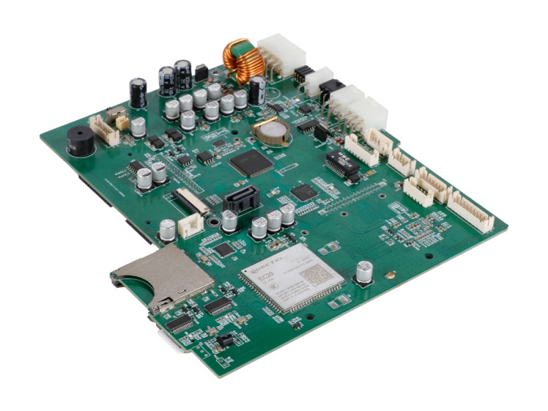
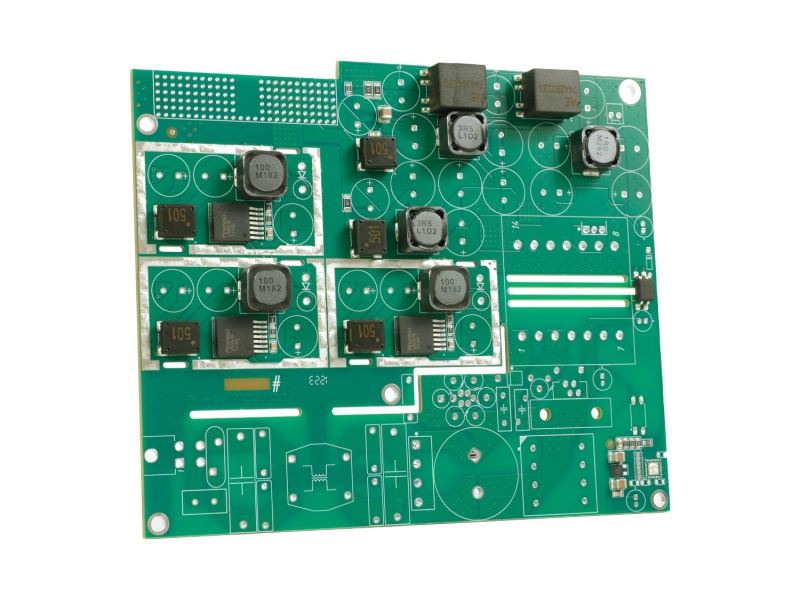
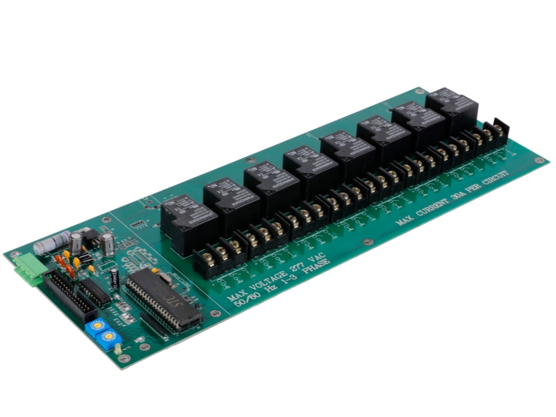
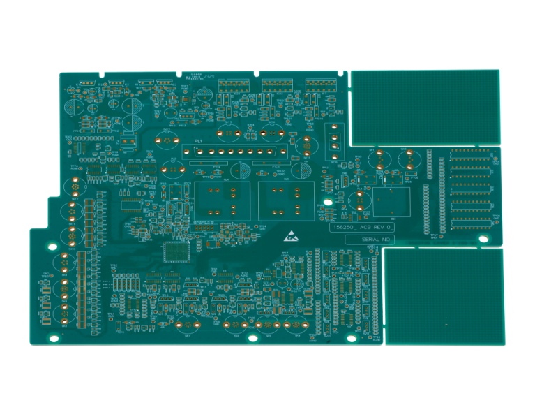
DQS Electronic Co., Limited has imported high-precision production equipment, with high-precision machinery, excellent metal base, ultra-thick copper production process, to create a first-class production line, to ensure the processing accuracy and quality. We can produce not only standar PCBs but difficult circuit board. Not ever how difficult, only send us your PCB file, our engineer can support your with good solution.
|
Item |
HDI PCB Capability |
|
Layer |
4-64 L |
| HDI Structure |
1+N+1, 2+N+2, 3+N+3 or any layer interconnection |
|
HDI AVI |
Blind through holes, buried through holes, staggered through holes, stacked through holes, skip through holes |
|
Min. Hole Size |
0.075mm |
|
Min. Line Width/Space |
Rigid PCBs: 2mil/2mil ; Flex PCBs0.025 / 0.025mm |
|
Dielectric Thickness |
Max:0.2mm ; Min:0.06mm |
|
HDI PCB Production Capability |
200000m²/month |
|
Inner copper thickness |
0.5-15oz or more |
|
Outer copper thickness |
0.5-10oz |
|
Surface Finish |
OSP HASL: SMD 40µ to 2000µ’, GND 30µ to 800µ’ ENIG: Au 1µ to 5µ’, Ni 80µ to 200µ’ Immersion Tin: 0.8µm to 1.2µm Immersion Silver: 0.15µm to 0.45µm Hard gold plating: Au 1µ to 50µ’, Ni 80µ to 200µ’ Peelable film: 5mil Carbon Ink: 0.3mil |

We are committed to building a world-leading circuit board assembly service brand, providing customers with the most reliable products and support, setting a benchmark in the industry and promoting the development of the electronics industry.

Our hours
24H


 IPv6 network supported